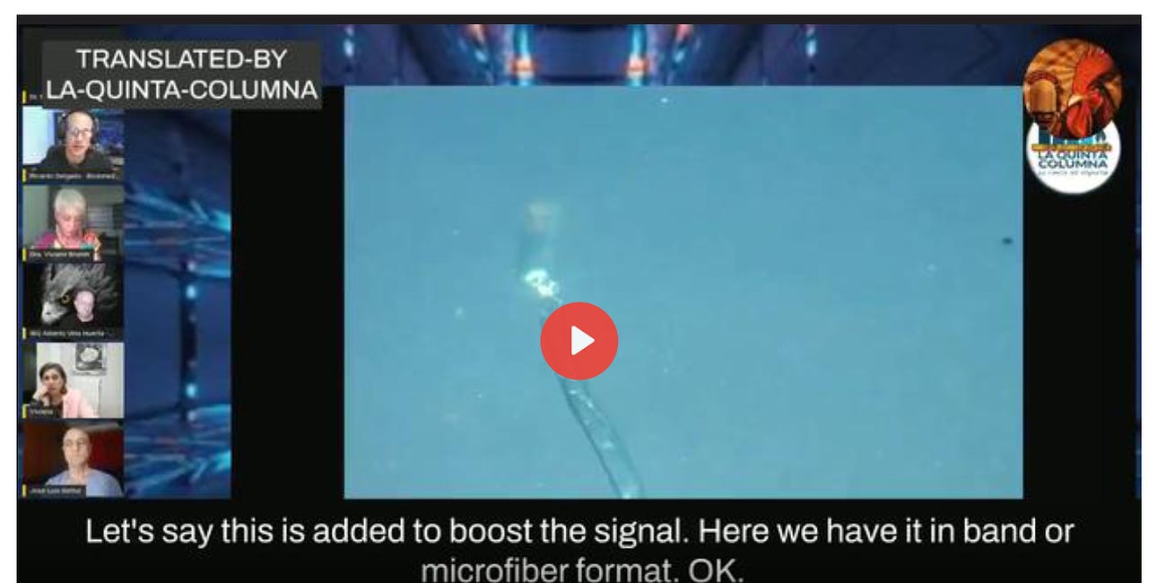
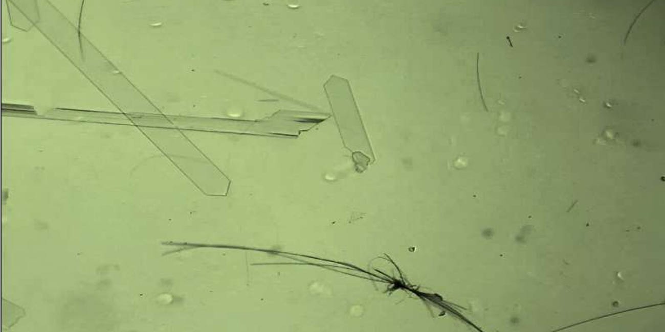
Let us briefly return to this area of science!
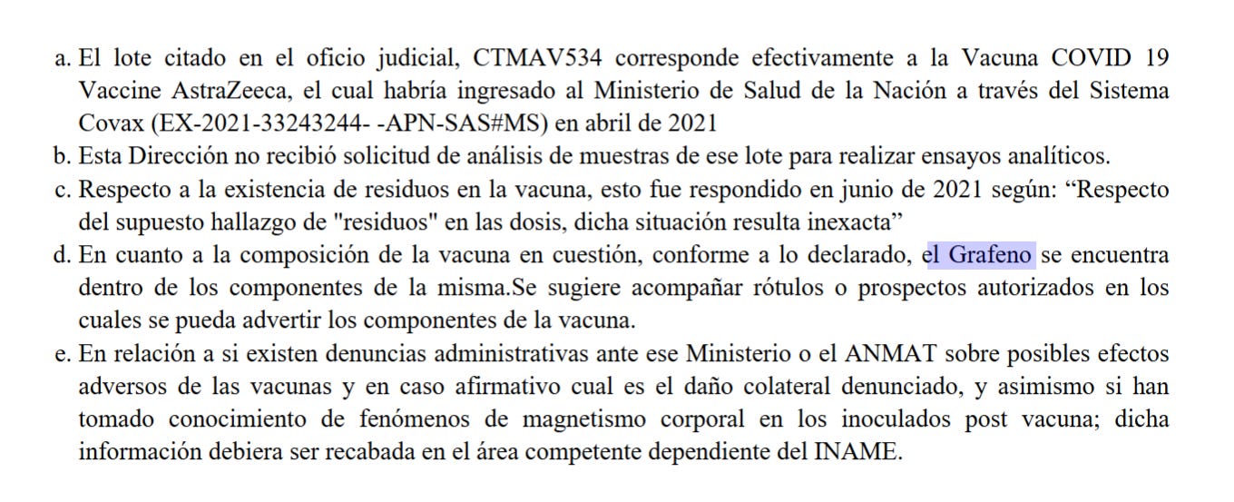
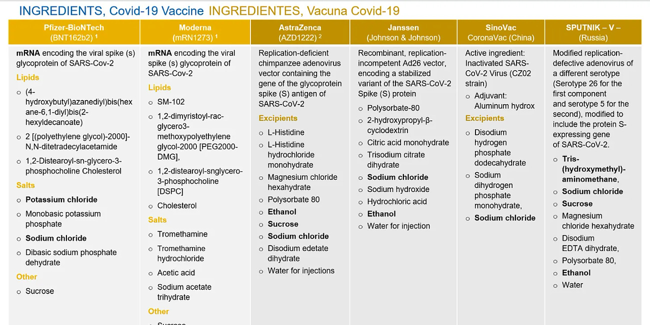
Dr. Patricia Aprea, Director of Evaluation and Control for ANMAT in Argentina, had ALREADY 2021 to admit on the record that the shots contain graphene!!!!!!
https://www.docdroid.net/lqjD2LT/if-2021-120912800-apn-decbranmat-pdf
What we also know:
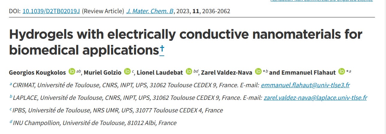
And everyone should and must assume that this is contained in all of these poison broths, because graphene/graphene oxide and its derivatives, together with hydrogel and other metallic nanoparticles, have excellent electrical conductivity!!
NOTE: People need to acquire knowledge in order to recognize the connections!
https://pubs.acs.org/doi/10.1021/acsnano.6b02313
https://www.researchgate.net/publication/301288013_Teslaphoresis_of_Carbon_Nanotubes
Nonuniform electric force fields are used to control the orientation, location, and assembly of a variety of nanoscale materials (e.g., carbon nanotubes, graphene, semiconducting quantum dots) for integration of their unique properties into electronic devices. (1-10) The force generated on particulate matter within a gradient electric field is a ponderomotive phenomenon known as dielectrophoresis, wherein neutral particles become polarized and migrate toward or away from regions of high electric field density. (11-13) Spatially varying electric force fields are traditionally created by fabricating two closely spaced (μm–mm) electrodes with appropriately shaped geometries resulting in a highly localized dielectrophoretic (DEP) force. (14-16) The magnitude of the DEP force generated in these systems is proportional to the gradient of the square of the electric field (FDEP ∝ ∇E2) and must be sufficiently strong to overcome Brownian motion. Although numerous DEP systems have been developed to manipulate nanoscale matter within these well-defined lithographically fabricated capacitor-like systems, these devices are inherently limited to the assembly of small scale volumes (μL–mL) and surface areas (μm2–cm2) due to the physical restrictions imposed by the two electrodes, which inhibit their use for scalable nanomanufacturing of materials and devices. (17, 18)
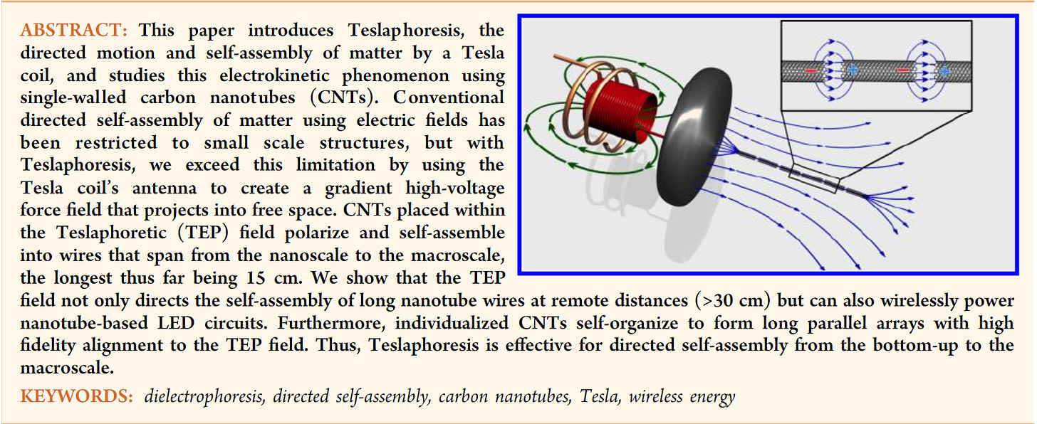
We have found that the physical limitations of conventional dielectrophoresis could be overcome by utilizing the near-field (≪ λ) radiofrequency (RF) energy transmitted by a Tesla coil. Although Nikola Tesla originally intended his namesake device to deliver wireless electrical energy around the world, (19) the Tesla coil proved to be impractical for radiative power transmission in the far-field (≫ λ), relegating the machine to be a relic of the late 19th century whose only purpose today is to create artificial lightning in science museums. (20) Nonetheless, the nonradiative, near-field region of a Tesla coil transmitter contains high intensity RF energy and this strong gradient electric field that extends into free space from the Tesla coil’s antenna can be harnessed to direct the self-assembly of nanoscale and macroscale particles over a long distance. Since the near-field region of a Tesla coil extends tens of meters away from the transmitter, we have found that the Tesla coil is remarkably capable of scalably moving, directing, and assembling particulate matter both on the nanoscale and the macroscale.
The directed motion and self-assembly of matter at a distance using the near-field energy of the Tesla coil is a phenomenon we term Teslaphoresis. We elected to use single-walled carbon nanotubes (CNTs) for this initial study because of their high polarizability, anisotropy, and the relative ease of studying the electrokinetic behavior of both bulk powders and individualized nanotubes in suspension. (21-23) When a small mass of CNT powder is placed within the near-field of the Tesla coil, explosive self-assembly and growth of an individual CNT wire occurs within a few seconds. If, instead, the CNTs are dispersed in solution, numerous nanotube wires begin to self-assemble rapidly and to combine into one or more larger parallel arrays. Furthermore, while Teslaphoresis has the distinct advantage of unrestricted directed self-assembly, we also found that the near-field energy of the Tesla coil wirelessly powers and self-assembles nanotube circuits and remotely self-assembles parallel arrays of individual nanotubes from the bottom-up.
Results and Discussion
Figure 1a illustrates our Teslaphoretic (TEP) system oriented horizontally to direct nanotube assembly into a wire on a surface. Traditional Tesla coils use high-voltage capacitors and spark-gaps to transmit broadband RF energy, while we designed our Tesla coil to be a narrowband amplitude-modulated RF transmitter continuously driven at its resonant frequency of 2 MHz by a plasma generator. The inductively coupled primary and secondary coils serve to amplify the RF signal from the generator and the resulting high voltage output from the coils directly feeds into a hollow disk-shaped antenna. (24) The near-field region surrounding the Tesla coil’s antenna is intrinsically a gradient quasi-static electric force field that can be precisely tuned by adjusting the power output from the plasma generator (minimum antenna potential of 10 kV with 5 W of transmitter power). Figure 1b shows results of our boundary element method (BEM) calculations for the quasi-static electric potential (E) and field lines of the antenna, whereas Figure 1c shows the corresponding function E2 and its gradient force field lines. The electric potential contours in Figure 1b drop 10% of the antenna voltage at each step, and are most closely spaced near the curved limits of the transmitting element in accord with the greater localized surface charge density there. Nearest the flat front surface of the antenna, the potential contours are close to parallel, and further away they spread spherically as the details of the antenna become unimportant compared to its total charge. Figure 1c shows that, as with two-plate capacitor DEP systems, the time-averaged TEP force is proportional to ∇E2. However, in our TEP system, the gradient electric field that gives rise to the TEP force is dominantly parallel to the symmetry axis of the system and is the region wherein all experiments were performed.
Figure 1. Teslaphoretic (TEP) system. (a) Schematic illustration of the TEP system consisting of a primary coil energized by a RF plasma generator (not shown) which creates a magnetic field (B-field) that inductively couples to the secondary coil, resulting in a high-voltage RF signal that terminates into a hollow disk-shaped antenna. The gradient electric field (E-field) projected into free space from the antenna creates a TEP force that polarizes and self-assembles carbon nanotubes into long wires. (b) BEM calculation of the quasi-static electric potential surrounding the antenna. The yellow lines represent equipotential contours and the red to blue color gradient represents the region of highest electric potential to the lowest, respectively. The green lines represent the electric force from the antenna along which the magnitude of the electric field decays. (c) BEM calculation of the TEP force field ∇E2 from the antenna (dashed green lines). The high-E2 region closest to the antenna has been clipped for clarity (white space). Each yellow equipotential line represents a 10% drop in E2 from the highest contour level that is not clipped (color gradient red to blue).
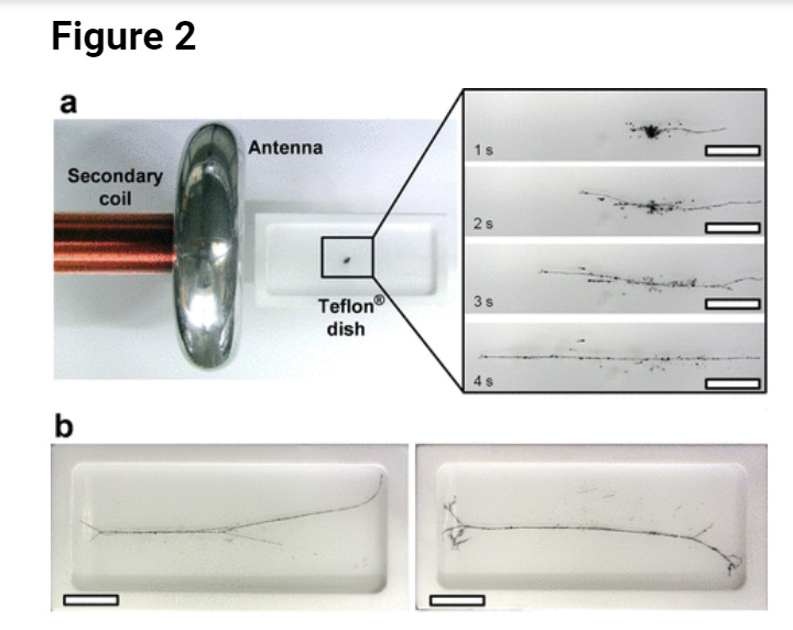
The magnified area in Figure 2a shows time-lapsed images of powdered CNTs (∼1 mg) self-assembling into a long thin wire in <5 s under a 30 W TEP field (Movie S1). The powdered nanotube particles were immersed in 20 mL of 1% Pluronic water in a Teflon dish and located 8 cm away from the surface of the antenna. Upon activating the TEP system, each particle quickly rotated and aligned its longest axis parallel to the direction of the electric field. The wire self-assembled at a remarkably rapid rate of 2 cm/s by sprouting nanotube fibrils on opposite sides of the central spot of the CNT powder, and these continuously grew both toward and away from the antenna until all particles were consumed into a single 10 cm long wire. Once fully grown, the wire then migrated toward the antenna at a rate of 0.5 cm/s until reaching the edge of the dish. These Teslaphoretically grown CNT wires are the longest directed self-assembled structures made to date, made possible because of the unconfined character of the TEP force field. (25, 26)
Movie S1 shows that numerous sparks within the nanotube wire occurred both during and after formation of the final assembled structure. These bright white sparks are similar to those observed in carbon arc lamps, and therefore, we predict that the heat generated from these regions would be equivalent. However, the heat released would be rapidly dissipated within the aqueous environment. In some instances, sparking was associated with dark plumes ejected from points along the wire. Optical absorption spectra of the expelled matter were featureless, indicating that it was likely carbonaceous material contained in the bulk CNT powder (whose automatic expulsion is desirable). Sparking within the wire indicates dielectric breakdown due to charge transfer that may originate from highly polarized metallic CNTs contained within the nanotube macroparticles. In considering the mechanism of growth, it is necessary to include not only the charge separations within particles, but also the transfer of charges between them. Interestingly, although dielectric breakdown during particle chaining was reported in early studies with conducting spheres, (27, 28) this direct observation of electric discharge has not been previously observed on such a large scale.
The TEP system is essentially a two-plate RF capacitor where the second plate is a virtual ground plane. (29) By replacing the virtual ground plane with a physical ground plane, we achieved directional control over the growth of the nanotube wire. Figure 2b shows that by placing an electrically grounded metal plate in proximity to the Teflon dish, the direction of growth of the distal end of the nanotube wire curves toward the grounded plate which was located 30 cm away from the antenna. The distal end consistently grew toward the grounded plate until the plate was moved farther than 50 cm from the antenna. The direction of growth always followed the electric field lines to the location of the grounded metal plate as evidenced by the curvature of the wires to opposite sides of the dish in the panels of Figure 2b. This faithful orientation of wire growth toward the nearest ground plane is a physical phenomenon similar to that for electrospun fibers and occurs even at minimum transmitter power. (30) Thus, the location of the ground plane is a critical factor in the TEP assembly process. Additionally, we found that the total length of the nanotube wire is linearly proportional to the amount of available nanotube mass.
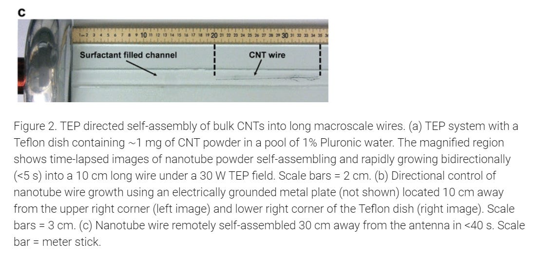
The theoretical range of the TEP force field is the entirety of the near-field region from the antenna, which for our system is over 20 m away. As shown in Figure 2c, one can grow much longer wires at remote distances by simply increasing the transmitter power (Movie S2). The 15 cm long nanotube wire rapidly self-assembled (∼40 s) 30 cm away from the antenna under a 100 W TEP field. The 5 mg spot of powdered CNTs was deposited within a 3 cm wide glass channel (containing 1% Pluronic water) parallel to the central axis of the disk-shaped antenna. Once fully formed, the entire wire rapidly accelerated toward the antenna at an initial rate of 1 cm/s. The speed of the wire could be controlled by reducing the transmitter power to a level that kept the wire taut yet stationary in front of the antenna. Upon deactivation of the TEP field, the wire remained assembled but relaxed in solution. Movie S3 shows the wire being broken apart with tweezers; then, upon reactivating the transmitter at low power (5 W), the fragments quickly realigned parallel to the direction of the electric field and self-assembled to heal the broken wire.
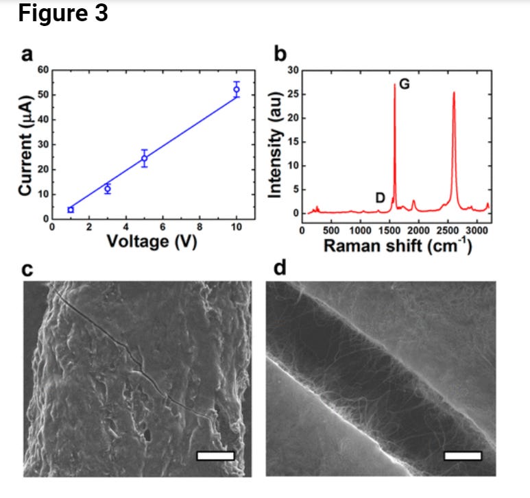
Figure 3 shows the electrical, structural, and morphological properties of our TEP assembled nanotube wire. The I–V curve in Figure 3a reveals that our nanotube wires exhibit remarkably consistent Ohmic behavior with a resistivity of 0.2 Ω·m. Figure 3b is a representative Raman spectrum of the wire with spectral features characteristic of single-walled carbon nanotubes including a sharp G-peak and an essentially absent D-peak indicating that our TEP field does not adversely affect the nanotube’s electronic structure. For scanning electron microscopy (SEM), the nanotubes were TEP-assembled in a solution of PMMA/ODCB (poly(methyl methacrylate)/o-dichlorobenzene) in order to preserve the wire for transfer onto a conductive substrate. Figure 3c shows a SEM image of a 150 μm diameter PMMA coated, TEP-assembled nanotube wire. The polymer obscured much of the substructure of the wire, but a diagonal fissure in the PMMA provided an uncoated region for higher magnification imaging. Figure 3d is a SEM of the region within the cracked polymer where we found randomly oriented, bundled nanotubes spanning the fissure and surrounding the gap.
The complex forces governing this bidirectional growth of the CNT wire are primarily due to the field-induced dipoles on individual CNT particles and the increasing strength of these dipoles as the nanotubes form chains. On the basis of our observations, the dominant driving force for the initial rapid growth is the generation of large charge separations along long conducting paths, which creates large induced dipole moments and strongly interacting local fields. Studies are underway to elaborate further on this mechanism, but it is clear that TEP assembly from a central source of particles is due to an interplay of forces wherein field-induced electrokinetics dominate and produce net growth along electric field lines. (31) When the CNT powder was dispersed throughout the solution instead of concentrated in a single spot, the TEP field rapidly directed the nanotubes into numerous parallel wires in solution across the entire Teflon dish (Movie S4). These macroscale arrays consist of many nanotubes, both end to end and in parallel, which collectively have well-established induced dipoles that follow the phase of the incident field. Consequently, further assembly throughout the solution into larger wires frequently occurs whenever the head of one CNT wire nears the oppositely charged tail of a nearby wire and they snap into head-to-tail contact.
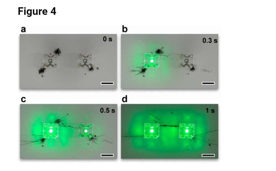
The near-field RF energy from the Tesla coil not only directs the self-assembly of long nanotube wires, but also wirelessly powers and self-assembles nanotube-based wet circuits. Figure 4 shows frames captured from Movie S5 of a pair of 4-pin green light-emitting diodes (LEDs) standing in a Teflon dish filled with 20 mL of 1% Pluronic water. Powdered CNTs (∼1 mg) were deposited next to the anode and cathode of LED 1 and the cathode alone of LED 2. Within 0.3 s of exposure to a 30 W TEP field, LED 1 was activated by the self-assembled nanotube wires that grew to the nearest cathode and anode. The CNT powder next to the cathode of LED 1 simultaneously grew both toward the antenna and toward the cathode. The CNT spot near the anode of LED 1 self-assembled and formed a CNT interconnect between both LEDs which then activated LED 2. As the wires elongated toward and away from the cathodes of their respective LED, more near-field energy was harvested by the nanotube wires resulting in an increasingly brighter emission from each LED in the circuit. By mapping the emission intensity from a single LED to a known current (Figure S1), we estimate that 1 μA was generated across these wires at low transmission power (5 W). This remarkable capability to simultaneously assemble and remotely power a wet circuit is a capability unique to the TEP method that has not been demonstrated with conventional DEP systems.
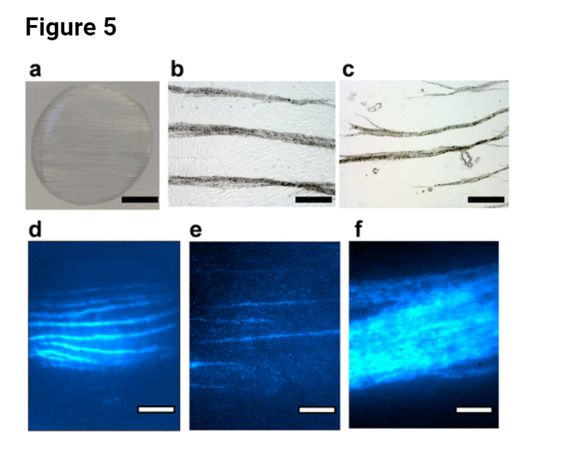
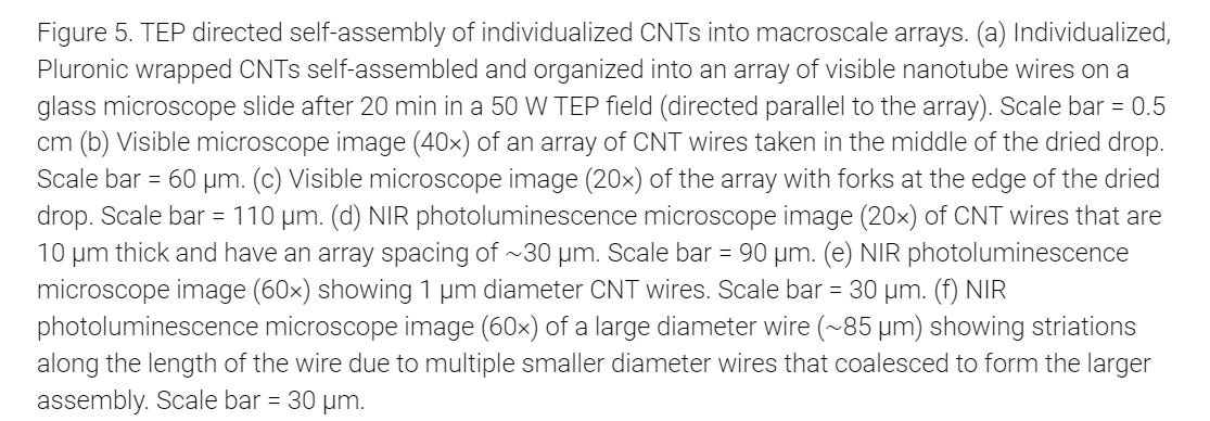
Finally, we studied the capability of the TEP system to direct the assembly of individualized nanotubes which were prepared by sonicating nanotube powder in 1% Pluronic water and then ultracentrifuging to remove the majority of bundles. (32) A 10 mg/L drop (50 μL) of the suspension enriched with individualized nanotubes (as evidenced by the near-infrared emission shown in Figure S2) was deposited onto a glass microscope slide located 3 cm away from the antenna. After a 20 min exposure to the 50 W TEP field, a dense array of very fine, parallel CNT wires emerged spanning across the diameter of the drop (Figure 5a, Movie S6). The drop was allowed to dry under ambient conditions with the TEP field active in order to preserve the organized array on the glass surface for microscopic analysis. Figure 5b is a 40× visible microscope image taken within the central region of the dried drop showing several parallel nanotube wires in the array (diameter = 25 μm, spacing = 60 μm). Variations in the nanotube wire diameter and in the spacing across the array are due to drying effects and coalescence of the nanotubes during growth. Figure 5c shows a 20× optical microscope image from the edge of the drop where we observed that all wires in the nanotube array were terminated by forks. This forked pattern is similar to that observed in electrical discharge phenomena such as lightning, plasma spheres, and Lichtenberg figures. (33)
Another significant finding was that even though these individual CNTs chained and coalesced into macroscale nanotube wires, they remained debundled within the wires due to the Pluronic coating surrounding each nanotube as evidenced by their persistent NIR emission. Figure 5d shows a NIR photoluminescence microscope image of a region within the center of the drop that contained smaller diameter nanotube wires (∼10 μm) and closer spacing (∼30 μm) than the wires in Figure 5b. The correlation between wire diameter and spacing is due to electrostatic repulsion from the parallel dipoles of the wires as they get thicker resulting in even stronger dipoles and farther spacing. (34) In addition, we observed several thin diameter nanotube wires (∼1 μm diameter) aligned with the electric field (Figure 5e) that were more easily observed through photoluminescence and were located between the larger diameter wires. These high aspect ratio wires could have only been formed from individual nanotubes self-assembling end-to-end as a means of maximizing their charge separation. This is further supported by the fact that when the polarized excitation was perpendicular to the long axis of the wire, the overall emission was reduced. Controlled growth of these very high aspect ratio wires can be optimized by precisely controlling the time, frequency and intensity of the applied TEP field. Both the visible and NIR microscope images show striations along the lengths of the wires that indicate strong alignment of neighboring nanotube chains within the larger structure. This is also highly evident in a 60× magnification NIR image of an 85 μm diameter wire (Figure 5f). SEM analysis (Figure S3) was also performed on the arrays in an effort to study the orientation of nanotubes within the TEP assembled wire. However, the Pluronic coating of the nanotubes obscured fine structure details of the assembled wire.
Additionally, a thin film nanotube suspension was prepared to reduce drying time, wherein we observed individual nanotubes aligning and attracted toward the tip of the growing nanotube wire (Figure S4). This is reminiscent of iron filings in magnetic fields or grass seeds in oil under electric fields providing evidence of the strong local fields between individual nanotubes and these larger structures. (35) Though the metal nanotubes are more susceptible to field alignment in this mixture, we have observed individual semiconducting nanotubes aligning with the field. Movie S7 shows a NIR microscopic scan across the nanotube wire array as the microscope stage was translated to follow a portion of the length of a wire.
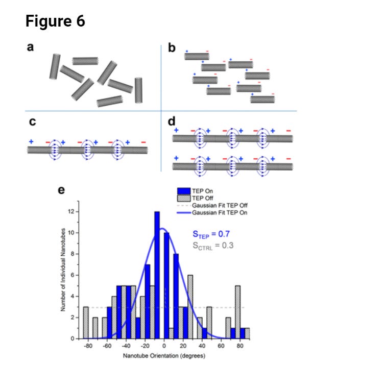
Figure 6a–d illustrates the mechanism of formation of CNT arrays from individual nanotubes under a TEP field. Prior to activation of the TEP field, nanotubes are individually suspended and randomly oriented in solution. When the TEP field is activated, the individual CNT particles are polarized and orient their long axis parallel to the direction of the electric field. The neighboring ends of CNTs with opposing dipoles undergo Columbic attraction and chain end-to-end, creating a long wire and increasing the separation of charge. Neighboring chains are held at a constant separation due to the electrostatic repulsion caused by the polarization charges at the ends of the CNT chains forming a uniform parallel array of nanotube wires from individual CNTs in suspension. These steps mirror those directly observed from macroscale CNT particles described earlier. It is interesting to note that the force of charge repulsion that spaces the wires is overcome when neighboring chains coalesce and form thicker wires as observed in Figure 5f. In this case, we have observed neighboring chains of wires joining when there is a break in the wire. The end of a nearby CNT chain is attracted to the strong gradient electric field within the broken wire and heals it, sweeping in the rest of the length of the chain to the surface of the adjacent wire. The chains merge and the cumulative charge is dispersed along the length of the new large chain (wire). Further evidence of this mechanism is seen in NIR emission images of the thin film where this process of alignment was preserved through rapid evaporation of the solution and the CNTs were seen to be attracted to an end of the larger diameter wire as mentioned for Figure S4.
The degree of alignment of individual nanotubes was quantified by utilizing the polarized NIR emission from individual nanotubes. Individual CNTs are very high-aspect ratio nanoparticles (∼1 nm × 500 nm) allowing us to utilize the polarization properties of the excitation laser to measure the degree of alignment of the nanotubes with the direction of the TEP field. (36) When the excitation polarization was parallel to the long axis of the nanotube, the emission intensity was maximized, whereas under perpendicular polarization, it was minimized. NIR images of TEP highly aligned nanotubes under two orthogonal polarizations exhibit this effect of maximum and minimum intensity as shown in Figure S5. The histogram in Figure 6e was plotted by measuring the intensity of individual nanotubes (located in the spacing between the larger diameter nanotube wires in the array) over a range of laser polarization angles and sinusoidally fitting the intensities to calculate each nanotube’s relative orientation with respect to the direction of the TEP field. These values were compared to a control sample placed in front of the system with the TEP system off. The histogram in Figure 6e shows that 64% of the “TEP field on” nanotubes were aligned within ±20° of the direction of the TEP field, whereas the control sample only had 17% alignment in the same range, a value consistent with a randomly distributed sample. Comparing the orientational order parameter (31)
of the TEP-exposed nanotubes vs the control nanotubes revealed that the former have an order parameter of 0.7, indicating strong alignment, whereas the latter again indicates random distribution with an order parameter of 0.3.
Conclusions
Although our study of TEP assembly has focused solely on carbon nanotubes, we have performed exploratory experiments with several other materials, and have observed their directed, scalable assembly. (37) In addition, our transmission frequency of 2 MHz was selected because nanotubes and their arrays are relatively insensitive to changes in this frequency range, but future work will explore the frequency dependence of TEP directed assemblies. (38-40) The intriguing capability of the TEP force to assemble and parallelize individual semiconductors on a surface en masse without any chemical template or lithography could lead to its application for the scalable fabrication of high-density parallel nanotubes in computer processors or possibly bottom-up assembly of conductive nanotube fibers as long as the near-field of the system (tens of meters). (41-45) In addition, our single antenna TEP system easily generalizes to multiple Tesla coils as a means to create more complex fields and structures thereby enabling even finer directional control over desired constructs. Therefore, the TEP system and methodology will become important tools in scalable nanomanufacturing, and the ability to interconnect, repair, and power circuit elements solely by using the near-field energy from the Tesla coil provides even greater prospects for the use of the TEP assembler beyond that of conventional dielectrophoresis.
Methods
TEP System
Figure S6 shows a circuit diagram of our 2 MHz TEP system. The primary of the Tesla coil was composed of hollow copper tubing (0.25 in. o.d.) fabricated by forming a 5-turn helical coil (5 in. diameter, 5 in. height, 0.25 in. pitch). The primary was conductively coupled to the output of a 2 MHz plasma generator (MKS Nova-25A, 2.5 kW RF Plasma Generator) and the remaining end of the coil was electrically grounded. The secondary coil was fabricated by tightly winding 18 AWG magnet wire around a hollow, polycarbonate cylinder (o.d. 2 in. ). One end of the secondary coil was conductively coupled to an 8 in. diameter aluminum toroid (Amazing 1, LLC) and the remaining end was electrically grounded. The toroid was capped with a 7.5 in. diameter aluminum disk to fabricate the 2 MHz Tesla coil’s antenna. The Tesla coil was positioned horizontally on an electrically insulated post and all samples were placed directly in front of the antenna on a nonconducting RF transparent platform. The transmission from the TEP system was maximized by matching the power of the activated Tesla coil.
TEP Directed CNT Assembly and Wirelessly Powered Nanotube-Based Circuits
The CNTs used in this study were powdered, purified, HiPco nanotubes (Rice University, HPR 162.8). CNT powder (1 or 5 mg) was placed in the center of the Teflon dish (6 × 15 cm2) or on the surface of the glass plate (0.1 × 1 m2). TEP directed assembly on the Teflon dish contained 20 mL of 1% Pluronic water and TEP assembly on glass plates were conducted within a long channel (3 cm × 1 m) containing 50 mL of 1% Pluronic water. All nanotubes were exposed to the TEP field until the formation of the assembled CNT wire was completed. Directional growth control was achieved by placing a grounded metal disk (6 in. diameter) at a 45° angle 30 cm away from the transmitting antenna on either the left or right side of the Teflon dish. The 4-pin green LEDs were rated 20 mA and the 4-pin red LED was rated 70 mA. Current values were mapped to intensity for the red LED using an adjustable DC power source and voltmeter. All visible movies and images were captured using a Canon HD video MF500 camera at 30 frames/s.
TEP Directed Self-Assembly of individual CNTs
A dispersed nanotube suspension was prepared by tip sonicating 10 mg CNTs in 100 mL of 1% (w/v) Pluronic F108 for 2 min at 70 W (Misonex Sonicator 3000). The suspension was centrifuged at 100 000g for 4 h prior to use, and 50 μL of the supernatant was transferred via pipet to a glass microscope slide. The drop was located 3 cm from the front surface of the antenna, and the TEP system was activated to 50 W. The drop dried at room temperature with the TEP field active until the solution evaporated. The slides were fitted with a glass coverslip and imaged on an inverted microscope (Nikon TE-2000U Eclipse) coupled to a Nikon DS-Fi1 camera for visible imaging or a Roper Scientific OMA-V:2D liquid-nitrogen-cooled InGaAs camera for NIR imaging. Additionally, for the control sample, a 50 μL drop of the same nanotube suspension was allowed to air-dry on a microscope slide with no applied TEP field. All NIR images were false-colored using hot cyan LUT in ImageJ to enhance the clarity of the fluorescence emission and were acquired with a 200 ms accumulation under a 840 nm laser excitation. To quantify the degree of individual CNT alignment by the TEP field, emission intensities from individual nanotubes were collected over a range of laser polarization angles (8° steps to cover 240° total) and fit to sine curves and angles calculated. (20) This calculation was performed on 58 nanotubes in a TEP aligned drop and 53 nanotubes from an air-dried drop of the same CNT suspension sample. The histograms were plotted and fit to a Gaussian function in Origin.
Characterization
NIR emission spectra were obtained with 660 nm excitation using a model NS1 NanoSpectralyzer (Applied NanoFluorescence, LLC). Bulk electrical resistivity measurements were performed on an ∼2 mg mass of CNTs self-assembled in 1% Pluronic water under a 5 W TEP field. The nanotubes self-assembled until making contact with two copper wires spaced 2 cm apart. The current drop across the nanotube wire was measured under a series of constant voltages (1–10 V) applied to the nanotube wire from a DC power supply. Raman spectra of the nanotube wire were acquired using a Renishaw Raman microscope with 633 nm excitation. For SEM imaging of the macroscale wire, directed self-assembly was performed on a mixture of polymeric solution of PMMA/ODCB nanotubes under a 50 W TEP field. The wire was removed from the polymer using tweezers and placed directly on a conductive substrate. SEM images were acquired using a FEI Quanta 400 ESEM operated in wet mode with 3 Torr water vapor at 10 kV. Pluronic coated nanotube arrays were sputter coated with a 5 nm layer of gold prior to SEM imaging using a Denton Desk V Sputter System.
Nonuniform electric force fields are used to control the orientation, location, and assembly of a variety of nanoscale materials (e.g., carbon nanotubes, graphene, semiconducting quantum dots) for integration of their unique properties into electronic devices. (1-10) The force generated on particulate matter within a gradient electric field is a ponderomotive phenomenon known as dielectrophoresis, wherein neutral particles become polarized and migrate toward or away from regions of high electric field density. (11-13) Spatially varying electric force fields are traditionally created by fabricating two closely spaced (μm–mm) electrodes with appropriately shaped geometries resulting in a highly localized dielectrophoretic (DEP) force. (14-16) The magnitude of the DEP force generated in these systems is proportional to the gradient of the square of the electric field (FDEP ∝ ∇E2) and must be sufficiently strong to overcome Brownian motion. Although numerous DEP systems have been developed to manipulate nanoscale matter within these well-defined lithographically fabricated capacitor-like systems, these devices are inherently limited to the assembly of small scale volumes (μL–mL) and surface areas (μm2–cm2) due to the physical restrictions imposed by the two electrodes, which inhibit their use for scalable nanomanufacturing of materials and devices. (17, 18)
We have found that the physical limitations of conventional dielectrophoresis could be overcome by utilizing the near-field (≪ λ) radiofrequency (RF) energy transmitted by a Tesla coil. Although Nikola Tesla originally intended his namesake device to deliver wireless electrical energy around the world, (19) the Tesla coil proved to be impractical for radiative power transmission in the far-field (≫ λ), relegating the machine to be a relic of the late 19th century whose only purpose today is to create artificial lightning in science museums. (20) Nonetheless, the nonradiative, near-field region of a Tesla coil transmitter contains high intensity RF energy and this strong gradient electric field that extends into free space from the Tesla coil’s antenna can be harnessed to direct the self-assembly of nanoscale and macroscale particles over a long distance. Since the near-field region of a Tesla coil extends tens of meters away from the transmitter, we have found that the Tesla coil is remarkably capable of scalably moving, directing, and assembling particulate matter both on the nanoscale and the macroscale.
The directed motion and self-assembly of matter at a distance using the near-field energy of the Tesla coil is a phenomenon we term Teslaphoresis. We elected to use single-walled carbon nanotubes (CNTs) for this initial study because of their high polarizability, anisotropy, and the relative ease of studying the electrokinetic behavior of both bulk powders and individualized nanotubes in suspension. (21-23) When a small mass of CNT powder is placed within the near-field of the Tesla coil, explosive self-assembly and growth of an individual CNT wire occurs within a few seconds. If, instead, the CNTs are dispersed in solution, numerous nanotube wires begin to self-assemble rapidly and to combine into one or more larger parallel arrays. Furthermore, while Teslaphoresis has the distinct advantage of unrestricted directed self-assembly, we also found that the near-field energy of the Tesla coil wirelessly powers and self-assembles nanotube circuits and remotely self-assembles parallel arrays of individual nanotubes from the bottom-up.
Results and Discussion
ARTICLE SECTIONS
Figure 1a illustrates our Teslaphoretic (TEP) system oriented horizontally to direct nanotube assembly into a wire on a surface. Traditional Tesla coils use high-voltage capacitors and spark-gaps to transmit broadband RF energy, while we designed our Tesla coil to be a narrowband amplitude-modulated RF transmitter continuously driven at its resonant frequency of 2 MHz by a plasma generator. The inductively coupled primary and secondary coils serve to amplify the RF signal from the generator and the resulting high voltage output from the coils directly feeds into a hollow disk-shaped antenna. (24) The near-field region surrounding the Tesla coil’s antenna is intrinsically a gradient quasi-static electric force field that can be precisely tuned by adjusting the power output from the plasma generator (minimum antenna potential of 10 kV with 5 W of transmitter power). Figure 1b shows results of our boundary element method (BEM) calculations for the quasi-static electric potential (E) and field lines of the antenna, whereas Figure 1c shows the corresponding function E2 and its gradient force field lines. The electric potential contours in Figure 1b drop 10% of the antenna voltage at each step, and are most closely spaced near the curved limits of the transmitting element in accord with the greater localized surface charge density there. Nearest the flat front surface of the antenna, the potential contours are close to parallel, and further away they spread spherically as the details of the antenna become unimportant compared to its total charge. Figure 1c shows that, as with two-plate capacitor DEP systems, the time-averaged TEP force is proportional to ∇E2. However, in our TEP system, the gradient electric field that gives rise to the TEP force is dominantly parallel to the symmetry axis of the system and is the region wherein all experiments were performed.
The magnified area in Figure 2a shows time-lapsed images of powdered CNTs (∼1 mg) self-assembling into a long thin wire in <5 s under a 30 W TEP field (Movie S1). The powdered nanotube particles were immersed in 20 mL of 1% Pluronic water in a Teflon dish and located 8 cm away from the surface of the antenna. Upon activating the TEP system, each particle quickly rotated and aligned its longest axis parallel to the direction of the electric field. The wire self-assembled at a remarkably rapid rate of 2 cm/s by sprouting nanotube fibrils on opposite sides of the central spot of the CNT powder, and these continuously grew both toward and away from the antenna until all particles were consumed into a single 10 cm long wire. Once fully grown, the wire then migrated toward the antenna at a rate of 0.5 cm/s until reaching the edge of the dish. These Teslaphoretically grown CNT wires are the longest directed self-assembled structures made to date, made possible because of the unconfined character of the TEP force field. (25, 26)
Movie S1 shows that numerous sparks within the nanotube wire occurred both during and after formation of the final assembled structure. These bright white sparks are similar to those observed in carbon arc lamps, and therefore, we predict that the heat generated from these regions would be equivalent. However, the heat released would be rapidly dissipated within the aqueous environment. In some instances, sparking was associated with dark plumes ejected from points along the wire. Optical absorption spectra of the expelled matter were featureless, indicating that it was likely carbonaceous material contained in the bulk CNT powder (whose automatic expulsion is desirable). Sparking within the wire indicates dielectric breakdown due to charge transfer that may originate from highly polarized metallic CNTs contained within the nanotube macroparticles. In considering the mechanism of growth, it is necessary to include not only the charge separations within particles, but also the transfer of charges between them. Interestingly, although dielectric breakdown during particle chaining was reported in early studies with conducting spheres, (27, 28) this direct observation of electric discharge has not been previously observed on such a large scale.
The TEP system is essentially a two-plate RF capacitor where the second plate is a virtual ground plane. (29) By replacing the virtual ground plane with a physical ground plane, we achieved directional control over the growth of the nanotube wire. Figure 2b shows that by placing an electrically grounded metal plate in proximity to the Teflon dish, the direction of growth of the distal end of the nanotube wire curves toward the grounded plate which was located 30 cm away from the antenna. The distal end consistently grew toward the grounded plate until the plate was moved farther than 50 cm from the antenna. The direction of growth always followed the electric field lines to the location of the grounded metal plate as evidenced by the curvature of the wires to opposite sides of the dish in the panels of Figure 2b. This faithful orientation of wire growth toward the nearest ground plane is a physical phenomenon similar to that for electrospun fibers and occurs even at minimum transmitter power. (30) Thus, the location of the ground plane is a critical factor in the TEP assembly process. Additionally, we found that the total length of the nanotube wire is linearly proportional to the amount of available nanotube mass.
The theoretical range of the TEP force field is the entirety of the near-field region from the antenna, which for our system is over 20 m away. As shown in Figure 2c, one can grow much longer wires at remote distances by simply increasing the transmitter power (Movie S2). The 15 cm long nanotube wire rapidly self-assembled (∼40 s) 30 cm away from the antenna under a 100 W TEP field. The 5 mg spot of powdered CNTs was deposited within a 3 cm wide glass channel (containing 1% Pluronic water) parallel to the central axis of the disk-shaped antenna. Once fully formed, the entire wire rapidly accelerated toward the antenna at an initial rate of 1 cm/s. The speed of the wire could be controlled by reducing the transmitter power to a level that kept the wire taut yet stationary in front of the antenna. Upon deactivation of the TEP field, the wire remained assembled but relaxed in solution. Movie S3 shows the wire being broken apart with tweezers; then, upon reactivating the transmitter at low power (5 W), the fragments quickly realigned parallel to the direction of the electric field and self-assembled to heal the broken wire.
Figure 3 shows the electrical, structural, and morphological properties of our TEP assembled nanotube wire. The I–V curve in Figure 3a reveals that our nanotube wires exhibit remarkably consistent Ohmic behavior with a resistivity of 0.2 Ω·m. Figure 3b is a representative Raman spectrum of the wire with spectral features characteristic of single-walled carbon nanotubes including a sharp G-peak and an essentially absent D-peak indicating that our TEP field does not adversely affect the nanotube’s electronic structure. For scanning electron microscopy (SEM), the nanotubes were TEP-assembled in a solution of PMMA/ODCB (poly(methyl methacrylate)/o-dichlorobenzene) in order to preserve the wire for transfer onto a conductive substrate. Figure 3c shows a SEM image of a 150 μm diameter PMMA coated, TEP-assembled nanotube wire. The polymer obscured much of the substructure of the wire, but a diagonal fissure in the PMMA provided an uncoated region for higher magnification imaging. Figure 3d is a SEM of the region within the cracked polymer where we found randomly oriented, bundled nanotubes spanning the fissure and surrounding the gap.
The complex forces governing this bidirectional growth of the CNT wire are primarily due to the field-induced dipoles on individual CNT particles and the increasing strength of these dipoles as the nanotubes form chains. On the basis of our observations, the dominant driving force for the initial rapid growth is the generation of large charge separations along long conducting paths, which creates large induced dipole moments and strongly interacting local fields. Studies are underway to elaborate further on this mechanism, but it is clear that TEP assembly from a central source of particles is due to an interplay of forces wherein field-induced electrokinetics dominate and produce net growth along electric field lines. (31) When the CNT powder was dispersed throughout the solution instead of concentrated in a single spot, the TEP field rapidly directed the nanotubes into numerous parallel wires in solution across the entire Teflon dish (Movie S4). These macroscale arrays consist of many nanotubes, both end to end and in parallel, which collectively have well-established induced dipoles that follow the phase of the incident field. Consequently, further assembly throughout the solution into larger wires frequently occurs whenever the head of one CNT wire nears the oppositely charged tail of a nearby wire and they snap into head-to-tail contact.
The near-field RF energy from the Tesla coil not only directs the self-assembly of long nanotube wires, but also wirelessly powers and self-assembles nanotube-based wet circuits. Figure 4 shows frames captured from Movie S5 of a pair of 4-pin green light-emitting diodes (LEDs) standing in a Teflon dish filled with 20 mL of 1% Pluronic water. Powdered CNTs (∼1 mg) were deposited next to the anode and cathode of LED 1 and the cathode alone of LED 2. Within 0.3 s of exposure to a 30 W TEP field, LED 1 was activated by the self-assembled nanotube wires that grew to the nearest cathode and anode. The CNT powder next to the cathode of LED 1 simultaneously grew both toward the antenna and toward the cathode. The CNT spot near the anode of LED 1 self-assembled and formed a CNT interconnect between both LEDs which then activated LED 2. As the wires elongated toward and away from the cathodes of their respective LED, more near-field energy was harvested by the nanotube wires resulting in an increasingly brighter emission from each LED in the circuit. By mapping the emission intensity from a single LED to a known current (Figure S1), we estimate that 1 μA was generated across these wires at low transmission power (5 W). This remarkable capability to simultaneously assemble and remotely power a wet circuit is a capability unique to the TEP method that has not been demonstrated with conventional DEP systems.
Finally, we studied the capability of the TEP system to direct the assembly of individualized nanotubes which were prepared by sonicating nanotube powder in 1% Pluronic water and then ultracentrifuging to remove the majority of bundles. (32) A 10 mg/L drop (50 μL) of the suspension enriched with individualized nanotubes (as evidenced by the near-infrared emission shown in Figure S2) was deposited onto a glass microscope slide located 3 cm away from the antenna. After a 20 min exposure to the 50 W TEP field, a dense array of very fine, parallel CNT wires emerged spanning across the diameter of the drop (Figure 5a, Movie S6). The drop was allowed to dry under ambient conditions with the TEP field active in order to preserve the organized array on the glass surface for microscopic analysis. Figure 5b is a 40× visible microscope image taken within the central region of the dried drop showing several parallel nanotube wires in the array (diameter = 25 μm, spacing = 60 μm). Variations in the nanotube wire diameter and in the spacing across the array are due to drying effects and coalescence of the nanotubes during growth. Figure 5c shows a 20× optical microscope image from the edge of the drop where we observed that all wires in the nanotube array were terminated by forks. This forked pattern is similar to that observed in electrical discharge phenomena such as lightning, plasma spheres, and Lichtenberg figures. (33)
Another significant finding was that even though these individual CNTs chained and coalesced into macroscale nanotube wires, they remained debundled within the wires due to the Pluronic coating surrounding each nanotube as evidenced by their persistent NIR emission. Figure 5d shows a NIR photoluminescence microscope image of a region within the center of the drop that contained smaller diameter nanotube wires (∼10 μm) and closer spacing (∼30 μm) than the wires in Figure 5b. The correlation between wire diameter and spacing is due to electrostatic repulsion from the parallel dipoles of the wires as they get thicker resulting in even stronger dipoles and farther spacing. (34) In addition, we observed several thin diameter nanotube wires (∼1 μm diameter) aligned with the electric field (Figure 5e) that were more easily observed through photoluminescence and were located between the larger diameter wires. These high aspect ratio wires could have only been formed from individual nanotubes self-assembling end-to-end as a means of maximizing their charge separation. This is further supported by the fact that when the polarized excitation was perpendicular to the long axis of the wire, the overall emission was reduced. Controlled growth of these very high aspect ratio wires can be optimized by precisely controlling the time, frequency and intensity of the applied TEP field. Both the visible and NIR microscope images show striations along the lengths of the wires that indicate strong alignment of neighboring nanotube chains within the larger structure. This is also highly evident in a 60× magnification NIR image of an 85 μm diameter wire (Figure 5f). SEM analysis (Figure S3) was also performed on the arrays in an effort to study the orientation of nanotubes within the TEP assembled wire. However, the Pluronic coating of the nanotubes obscured fine structure details of the assembled wire.
Additionally, a thin film nanotube suspension was prepared to reduce drying time, wherein we observed individual nanotubes aligning and attracted toward the tip of the growing nanotube wire (Figure S4). This is reminiscent of iron filings in magnetic fields or grass seeds in oil under electric fields providing evidence of the strong local fields between individual nanotubes and these larger structures. (35) Though the metal nanotubes are more susceptible to field alignment in this mixture, we have observed individual semiconducting nanotubes aligning with the field. Movie S7 shows a NIR microscopic scan across the nanotube wire array as the microscope stage was translated to follow a portion of the length of a wire.
Figure 6a–d illustrates the mechanism of formation of CNT arrays from individual nanotubes under a TEP field. Prior to activation of the TEP field, nanotubes are individually suspended and randomly oriented in solution. When the TEP field is activated, the individual CNT particles are polarized and orient their long axis parallel to the direction of the electric field. The neighboring ends of CNTs with opposing dipoles undergo Columbic attraction and chain end-to-end, creating a long wire and increasing the separation of charge. Neighboring chains are held at a constant separation due to the electrostatic repulsion caused by the polarization charges at the ends of the CNT chains forming a uniform parallel array of nanotube wires from individual CNTs in suspension. These steps mirror those directly observed from macroscale CNT particles described earlier. It is interesting to note that the force of charge repulsion that spaces the wires is overcome when neighboring chains coalesce and form thicker wires as observed in Figure 5f. In this case, we have observed neighboring chains of wires joining when there is a break in the wire. The end of a nearby CNT chain is attracted to the strong gradient electric field within the broken wire and heals it, sweeping in the rest of the length of the chain to the surface of the adjacent wire. The chains merge and the cumulative charge is dispersed along the length of the new large chain (wire). Further evidence of this mechanism is seen in NIR emission images of the thin film where this process of alignment was preserved through rapid evaporation of the solution and the CNTs were seen to be attracted to an end of the larger diameter wire as mentioned for Figure S4.
The degree of alignment of individual nanotubes was quantified by utilizing the polarized NIR emission from individual nanotubes. Individual CNTs are very high-aspect ratio nanoparticles (∼1 nm × 500 nm) allowing us to utilize the polarization properties of the excitation laser to measure the degree of alignment of the nanotubes with the direction of the TEP field. (36) When the excitation polarization was parallel to the long axis of the nanotube, the emission intensity was maximized, whereas under perpendicular polarization, it was minimized. NIR images of TEP highly aligned nanotubes under two orthogonal polarizations exhibit this effect of maximum and minimum intensity as shown in Figure S5. The histogram in Figure 6e was plotted by measuring the intensity of individual nanotubes (located in the spacing between the larger diameter nanotube wires in the array) over a range of laser polarization angles and sinusoidally fitting the intensities to calculate each nanotube’s relative orientation with respect to the direction of the TEP field. These values were compared to a control sample placed in front of the system with the TEP system off. The histogram in Figure 6e shows that 64% of the “TEP field on” nanotubes were aligned within ±20° of the direction of the TEP field, whereas the control sample only had 17% alignment in the same range, a value consistent with a randomly distributed sample. Comparing the orientational order parameter (31)

of the TEP-exposed nanotubes vs the control nanotubes revealed that the former have an order parameter of 0.7, indicating strong alignment, whereas the latter again indicates random distribution with an order parameter of 0.3.
Conclusions
ARTICLE SECTIONS
Although our study of TEP assembly has focused solely on carbon nanotubes, we have performed exploratory experiments with several other materials, and have observed their directed, scalable assembly. (37) In addition, our transmission frequency of 2 MHz was selected because nanotubes and their arrays are relatively insensitive to changes in this frequency range, but future work will explore the frequency dependence of TEP directed assemblies. (38-40) The intriguing capability of the TEP force to assemble and parallelize individual semiconductors on a surface en masse without any chemical template or lithography could lead to its application for the scalable fabrication of high-density parallel nanotubes in computer processors or possibly bottom-up assembly of conductive nanotube fibers as long as the near-field of the system (tens of meters). (41-45) In addition, our single antenna TEP system easily generalizes to multiple Tesla coils as a means to create more complex fields and structures thereby enabling even finer directional control over desired constructs. Therefore, the TEP system and methodology will become important tools in scalable nanomanufacturing, and the ability to interconnect, repair, and power circuit elements solely by using the near-field energy from the Tesla coil provides even greater prospects for the use of the TEP assembler beyond that of conventional dielectrophoresis.
Methods
ARTICLE SECTIONS
TEP System
Figure S6 shows a circuit diagram of our 2 MHz TEP system. The primary of the Tesla coil was composed of hollow copper tubing (0.25 in. o.d.) fabricated by forming a 5-turn helical coil (5 in. diameter, 5 in. height, 0.25 in. pitch). The primary was conductively coupled to the output of a 2 MHz plasma generator (MKS Nova-25A, 2.5 kW RF Plasma Generator) and the remaining end of the coil was electrically grounded. The secondary coil was fabricated by tightly winding 18 AWG magnet wire around a hollow, polycarbonate cylinder (o.d. 2 in. ). One end of the secondary coil was conductively coupled to an 8 in. diameter aluminum toroid (Amazing 1, LLC) and the remaining end was electrically grounded. The toroid was capped with a 7.5 in. diameter aluminum disk to fabricate the 2 MHz Tesla coil’s antenna. The Tesla coil was positioned horizontally on an electrically insulated post and all samples were placed directly in front of the antenna on a nonconducting RF transparent platform. The transmission from the TEP system was maximized by matching the power of the activated Tesla coil.
TEP Directed CNT Assembly and Wirelessly Powered Nanotube-Based Circuits
The CNTs used in this study were powdered, purified, HiPco nanotubes (Rice University, HPR 162.8). CNT powder (1 or 5 mg) was placed in the center of the Teflon dish (6 × 15 cm2) or on the surface of the glass plate (0.1 × 1 m2). TEP directed assembly on the Teflon dish contained 20 mL of 1% Pluronic water and TEP assembly on glass plates were conducted within a long channel (3 cm × 1 m) containing 50 mL of 1% Pluronic water. All nanotubes were exposed to the TEP field until the formation of the assembled CNT wire was completed. Directional growth control was achieved by placing a grounded metal disk (6 in. diameter) at a 45° angle 30 cm away from the transmitting antenna on either the left or right side of the Teflon dish. The 4-pin green LEDs were rated 20 mA and the 4-pin red LED was rated 70 mA. Current values were mapped to intensity for the red LED using an adjustable DC power source and voltmeter. All visible movies and images were captured using a Canon HD video MF500 camera at 30 frames/s.
TEP Directed Self-Assembly of individual CNTs
A dispersed nanotube suspension was prepared by tip sonicating 10 mg CNTs in 100 mL of 1% (w/v) Pluronic F108 for 2 min at 70 W (Misonex Sonicator 3000). The suspension was centrifuged at 100 000g for 4 h prior to use, and 50 μL of the supernatant was transferred via pipet to a glass microscope slide. The drop was located 3 cm from the front surface of the antenna, and the TEP system was activated to 50 W. The drop dried at room temperature with the TEP field active until the solution evaporated. The slides were fitted with a glass coverslip and imaged on an inverted microscope (Nikon TE-2000U Eclipse) coupled to a Nikon DS-Fi1 camera for visible imaging or a Roper Scientific OMA-V:2D liquid-nitrogen-cooled InGaAs camera for NIR imaging. Additionally, for the control sample, a 50 μL drop of the same nanotube suspension was allowed to air-dry on a microscope slide with no applied TEP field. All NIR images were false-colored using hot cyan LUT in ImageJ to enhance the clarity of the fluorescence emission and were acquired with a 200 ms accumulation under a 840 nm laser excitation. To quantify the degree of individual CNT alignment by the TEP field, emission intensities from individual nanotubes were collected over a range of laser polarization angles (8° steps to cover 240° total) and fit to sine curves and angles calculated. (20) This calculation was performed on 58 nanotubes in a TEP aligned drop and 53 nanotubes from an air-dried drop of the same CNT suspension sample. The histograms were plotted and fit to a Gaussian function in Origin.
Characterization
NIR emission spectra were obtained with 660 nm excitation using a model NS1 NanoSpectralyzer (Applied NanoFluorescence, LLC). Bulk electrical resistivity measurements were performed on an ∼2 mg mass of CNTs self-assembled in 1% Pluronic water under a 5 W TEP field. The nanotubes self-assembled until making contact with two copper wires spaced 2 cm apart. The current drop across the nanotube wire was measured under a series of constant voltages (1–10 V) applied to the nanotube wire from a DC power supply. Raman spectra of the nanotube wire were acquired using a Renishaw Raman microscope with 633 nm excitation. For SEM imaging of the macroscale wire, directed self-assembly was performed on a mixture of polymeric solution of PMMA/ODCB nanotubes under a 50 W TEP field. The wire was removed from the polymer using tweezers and placed directly on a conductive substrate. SEM images were acquired using a FEI Quanta 400 ESEM operated in wet mode with 3 Torr water vapor at 10 kV. Pluronic coated nanotube arrays were sputter coated with a 5 nm layer of gold prior to SEM imaging using a Denton Desk V Sputter System.
Supporting Information
The Supporting Information is available free of charge on the ACS Publications website at DOI: 10.1021/acsnano.6b02313.
Additional experimental data (PDF)
Movie S1 (MPG)
Movie S2 (MPG)
Movie S3 (MPG)
Movie S4 (MPG)
Movie S5 (MPG)
Movie S6 (MPG)
Movie S7 (MPG)
With all my thoughts to you all!!!♥️♥️♥️


